- 您现在的位置:买卖IC网 > Sheet目录324 > EK-V6-ML631-G-J (Xilinx Inc)VIRTEX-6 HXT FPGA ML631 EVAL KIT
�� �
�
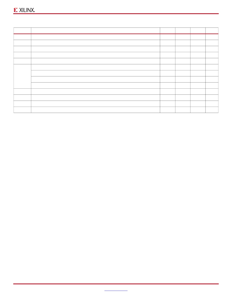
�Virtex-6� FPGA� Data� Sheet:� DC� and� Switching� Characteristics�
�Table� 3:� DC� Characteristics� Over� Recommended� Operating� Conditions� (1)(2)�
�Symbol�
�V� DRINT�
�V� DRI�
�I� REF�
�I� L�
�C� IN� (3)�
�I� RPU�
�I� RPD�
�I� BATT�
�n�
�r�
�Description�
�Data� retention� V� CCINT� voltage� (below� which� configuration� data� might� be� lost)�
�Data� retention� V� CCAUX� voltage� (below� which� configuration� data� might� be� lost)�
�V� REF� leakage� current� per� pin�
�Input� or� output� leakage� current� per� pin� (sample-tested)�
�Die� input� capacitance� at� the� pad�
�Pad� pull-up� (when� selected)� @� V� IN� =� 0V,� V� CCO� =� 2.5V�
�Pad� pull-up� (when� selected)� @� V� IN� =� 0V,� V� CCO� =� 1.8V�
�Pad� pull-up� (when� selected)� @� V� IN� =� 0V,� V� CCO� =� 1.5V�
�Pad� pull-up� (when� selected)� @� V� IN� =� 0V,� V� CCO� =� 1.2V�
�Pad� pull-down� (when� selected)� @� V� IN� =� 2.5V�
�Battery� supply� current�
�Temperature� diode� ideality� factor�
�Series� resistance�
�Min�
�0.75�
�2.0�
�–�
�–�
�–�
�20�
�8�
�5�
�1�
�3�
�–�
�–�
�–�
�Typ�
�–�
�–�
�–�
�–�
�–�
�–�
�–�
�–�
�–�
�–�
�–�
�1.0002�
�5�
�Max�
�–�
�–�
�10�
�10�
�8�
�80�
�40�
�30�
�20�
�80�
�150�
�–�
�–�
�Units�
�V�
�V�
�μA�
�μA�
�pF�
�μA�
�μA�
�μA�
�μA�
�μA�
�nA�
�n�
�Ω�
�Notes:�
�1.�
�2.�
�3.�
�Typical� values� are� specified� at� nominal� voltage,� 25°C.�
�Maximum� value� specified� for� worst� case� process� at� 25°C.�
�This� measurement� represents� the� die� capacitance� at� the� pad,� not� including� the� package.�
�DS152� (v3.6)� March� 18,� 2014�
�Product� Specification�
��3�
�发布紧急采购,3分钟左右您将得到回复。
相关PDF资料
EK-V7-VC707-CES-G
VIRTEX-7 VC707 EVAL KIT
EK-Z7-ZC702-CES-G
ZYNQ-7000 EPP ZC702 EVAL KIT
EL1848IYZ-T7
IC LED DRIVR WHITE BCKLGT 8-MSOP
EL7156CSZ
IC DRIVER PIN 40MHZ 3STATE 8SOIC
EL7158ISZ
IC DVR PIN 40MHZ 3STATE 8-SOIC
EL7222CSZ
IC DVR HS DUAL MOSFET 8-SOIC
EL7242CSZ
IC DVR HS DUAL MOSFET 8-SOIC
EL7243CMZ-T13
IC CCD DRIVER DUAL HS 20-SOIC
相关代理商/技术参数
EK-V7-VC707-CES-G
功能描述:VIRTEX-7 VC707 EVAL KIT RoHS:是 类别:编程器,开发系统 >> 通用嵌入式开发板和套件(MCU、DSP、FPGA、CPLD等) 系列:Virtex®-7 标准包装:1 系列:PICDEM™ 类型:MCU 适用于相关产品:PIC10F206,PIC16F690,PIC16F819 所含物品:板,线缆,元件,CD,PICkit 编程器 产品目录页面:659 (CN2011-ZH PDF)
EK-V7-VC707-CES-G-J
功能描述:VIRTEX-7 VC707 EVAL KIT JAPAN RoHS:是 类别:编程器,开发系统 >> 通用嵌入式开发板和套件(MCU、DSP、FPGA、CPLD等) 系列:Virtex®-7 标准包装:1 系列:PICDEM™ 类型:MCU 适用于相关产品:PIC10F206,PIC16F690,PIC16F819 所含物品:板,线缆,元件,CD,PICkit 编程器 产品目录页面:659 (CN2011-ZH PDF)
EK-V7-VC707-G
制造商:Xilinx 功能描述:VIRTEX-7 FPGA VC707 EVALUATION KIT - Boxed Product (Development Kits) 制造商:Xilinx 功能描述:KIT EVAL VIRTEX7 VC707 制造商:Xilinx 功能描述:VIRTEX-7 VC707 FPGA EVAL KIT
EK-V7-VC707-G-J
制造商:Xilinx 功能描述:KIT EVAL VIRTEX7 VC707 JAPAN
EKWF111
功能描述:WiFi/802.11开发工具 WF111 SDIO Eval kit
RoHS:否 制造商:Roving Networks 产品:Evaluation Boards 工具用于评估:RN-171 支持协议:802.11 b/g 频率:2.4 GHz 接口类型:UART 工作电源电压:2 V to 16 V
EKWT11-A
功能描述:蓝牙/802.15.1 开发工具 EKWT11-A
RoHS:否 制造商:Panasonic Electronic Components 产品:Bluetooth Evaluation Kit 工具用于评估:PAN1721 频率:2.4 GHz 接口类型:I2C 工作电源电压:2 V to 3.6 V
EKWT11-E
功能描述:蓝牙/802.15.1 开发工具 EKWT11-E
RoHS:否 制造商:Panasonic Electronic Components 产品:Bluetooth Evaluation Kit 工具用于评估:PAN1721 频率:2.4 GHz 接口类型:I2C 工作电源电压:2 V to 3.6 V
EKWT11i-A
功能描述:蓝牙/802.15.1 开发工具 WT11i A Eval Kit
RoHS:否 制造商:Panasonic Electronic Components 产品:Bluetooth Evaluation Kit 工具用于评估:PAN1721 频率:2.4 GHz 接口类型:I2C 工作电源电压:2 V to 3.6 V